Emerging applications ranging from AI for IoT, embedded vision, hardware security, 5G communications, and industrial/automotive automation are redefining hardware requirements for developers designing products that operate at the network Edge. In order to support these applications, Edge devices need:
- Low power consumption
- High performance
- High reliability
- Small form factor
To address these needs, Lattice has chosen to use 28 nm Fully Depleted Silicon-on-Insulator (FD-SOI) process technology for a new product family. Developed by Samsung, this process is similar to the bulk CMOS used to manufacture most semiconductors, yet enables previously-unseen reductions in device size and power consumption, while greatly improving performance and reliability. Lattice has also developed a new FPGA fabric architecture that reduces power consumption and FPGA form factor even further, yet still increases system performance. This combination of new manufacturing process and new FPGA fabric has resulted in the Lattice Nexus™ FPGA development platform.
Accelerating AI Processing Performance
To support emerging technologies at the network Edge like AI, device developers need to make their systems smarter. They are trying to achieve this by integrating more intelligence into their system to allow Edge devices to perform some real-time data processing and analysis at the Edge. The challenge for AI designers is that AI inferencing algorithms are very compute-intensive and require large blocks of memory to store values locally for computation. Historically, when AI solution developers required high levels of DSP to implement an algorithm, they went off-chip to find it – either to another processor in the system or to the cloud. The need to perform AI calculations off-chip can cause issues with data latency, and raises concerns around data privacy and security.
With the Nexus FPGA platform, Lattice addresses the latency problem by integrating larger blocks of RAM and optimizing DSP blocks so they can store data and perform computations locally. As a consequence, developers can implement AI inferencing algorithms at the Edge as Nexus FPGAs deliver twice the performance of earlier Lattice FPGAs – while consuming only half the power.
High Reliability
Lattice Nexus FPGAs not only support soft error correction (SEC) and error code correction (ECC) blocks, but also benefit from a thin oxide layer that protects every transistor in the FPGA from the effects of particle strikes to the substrate. As a result, FPGAs developed on the Lattice Nexus platform deliver a 100x improvement in soft error rates in comparison to competing FPGAs of a similar class.
Enabling Small Form Factors
The Lattice Nexus platform also addresses the need for ever-shrinking form factors in Edge devices. As other FPGA vendors design their products for data analysis applications in datacenters, their products feature larger architectures that scale poorly to the number of logic cells typical in a small FPGA. Lattice drew on its expertise developing small, low power FPGAs to create a compact FPGA architecture that enables devices with a physical footprint up to ten times smaller than competing FPGAs of similar logic density.
 Full System Solutions
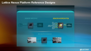
Lattice has created, or sourced and verified, easy-to-use, intuitive design software and pre-engineered soft IP blocks, evaluation boards, kits, and complete reference designs to enable fast and simple applications development.
The sensor aggregation demo Figure 1 shows how these demos help customers get products to market quickly. Targeted for use in embedded vision systems, the demo takes video data streams from up to four sources, combines them into a single stream, and then forwards that stream over a fast MIPI D-PHY to a display or processor for additional processing. Potential applications include advanced driver-assistance systems (ADAS) where developers need to collect data from multiple cameras and/or radar sensors, aggregate the data and then forward it to a processor to make safety decisions in real time. By eliminating the need to connect multiple sensors to the car’s AP, developers can reduce system cost and overall size by cutting the number of traces on the system’s PCB and conserving valuable AP I/O ports.
 The First Lattice Nexus FPGA: CrossLink-NX
Based on Lattice’s popular CrossLink family of FPGAs for video signal bridging, splitting and aggregation, the new CrossLink-NX™ FPGA family is the first of four planned FPGA families to be designed on the Lattice Nexus platform. CrossLink-NX supports all of the same video signal applications as the original device. The CrossLink-NX FPGA family’s higher memory-to-logic ratio, optimized DSPs, larger logic capacity and faster I/Os can process video data using AI algorithms while running twice as fast as previous FPGAs. Reliability is improved with up to a 100X reduction in SERs in a form factor up to 10X smaller than previous parts. The Diamond 2.0 FPGA development tool, proven IP blocks, and reference designs accelerate time-to-market.
