In semiconductor fabrication, the traditional approach to dry etching has been to utilise RF plasma to bombard the surface of the wafer with positive ions to remove material between masking layers.
Although ion etching has been effective for decades, it fails to produce the precise, sharp, nano-sized structures and pathways required in next generation devices. The process also generates significant amounts of heat that can damage underlying material layers, and for compound semiconductor materials such as GaN or SiC, it can change the surface atomic ratios.
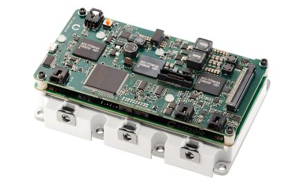
Now, in a move that goes against the grain of established traditional views of etching, VelvETch, together with PVA TePla America, have commercialised a new system with an approach called Electron Enhanced Material Processing (EEMP) that utilises the power of electrons – not ions – to much more precisely remove material at the nano-level.
In EEMP, precisely controlled waves of electrons are accelerated to the surface of the material at specific voltages designed to create chemical reactions that release the surface atomic bonds, allowing the material at the surface of the sample to be gently lifted away. The full-scale immersion by electrons allows the item being processed, such as a wafer, to be completed at an etch rate comparable to RF plasma etching.
Electron Etching
According to Samir Anz, he has been hearing “Electrons don’t etch” for decades, “but this is far from the case.”
“This is not an electron-beam scanning technology,” adds the co-founder of VelvETch, the company that developed the EEMP technology: “We emphasise this because when people hear ‘electrons’, they think ‘electron beam.’ This is a full-scale immersion technology. The entire semiconductor wafer or substrate is processed at all points, at the same time.”
However, with EEMP it is not the impact that drives the etching – rather, it is a chemical reaction induced by a loss of electrons from the bonds at the surface that causes surface atoms to be gently released, explains William A. Goddard III, an expert in theory of chemical and materials reactions and professor of chemistry, materials science, and applied physics at Caltech.
“We developed a way to study this process using quantum mechanics, and discovered that electrons in the discharge with the proper energy can remove an electron buried deep inside the atom, which in turn is filled with an electron from a bond while simultaneously knocking a second electron out of a bond,” explains Goddard. “When you lose two electrons from a bond, it breaks.” This is called an Auger event. “Since Auger processes occur only at the surface, EEMP leads to extremely smooth surfaces.”
Now commercialised by VelvETch after decades of research and development, EEMP is conducted in a jointly designed advanced plasma system platform provided by PVA TePla America, utilising a proprietary bias waveform signal that pulls the electrons down to the surface being processed.
Plasma Etching
In the traditional approach, plasma is created by applying a radio frequency signal (typically 13.56 MHz) that causes the atoms or molecules of the gases introduced into the chamber to increase in temperature until they ionsze into a plasma. A separately controlled radio frequency signal under the wafer pulls the positive ions down in a virtual “atomic sandblasting” of the surface of the material.
Due to the mostly vertical delivery of reactive ions, RF plasma etching can produce anisotropic etching useful to fabricate relatively sharp corners, flat surfaces and deep cavities. However, “When ions with over 1000 volts of energy hit the surface,” explains Professor Goddard, “You get a couple of nanometers of damage automatically, even in the best case.” This creates significant problems as transistors are miniaturised to ten nanometers and less. Moreover, ions that impact the surface with enough force to etch can be embedded several layers deep, causing electronic damage along with backscatter.
Compound Semiconductor Materials
Compound semiconductor materials are comprised of more than one element. Current high bandgap compound semiconductors include gallium nitride, gallium arsenide and silicon carbide.
“With gallium nitride, ion etching tends to remove nitrogen faster than gallium, leading to a gallium-rich surface with poor electrical properties,” explains Stewart Sando, a co-founder of VelvETch. Consequently, to eliminate excess gallium, wafers are often dipped in wet chemistry to restore the proper ratio of elements at the surface, hardly appropriate for new generation nanoscale devices. EEMP preserves the stoichiometry of compound semiconductors by carefully controlling the energy of the electrons in the discharge.
This advantage of EEMP also applies to quantum well structures, which sandwich a thin layer of one semiconductor between two layers of another semiconductor material with a wider band gap. Examples include aluminum gallium arsenide that confines the electrons to a gallium arsenide region, as well as indium gallium arsenide and gallium arsenide.
For more information on PVA TePla America, click here. Alternatively, contact sfsando@velvetch.com for more details.